(Hong Kong)

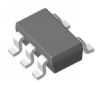
Product Summary
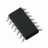
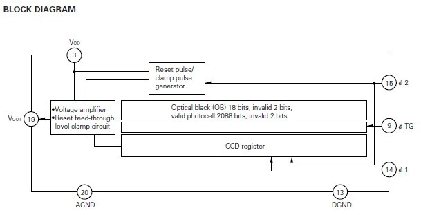
The UPD3753CY is a 2088-bit high sensitivity CCD (Charge Coupled Device) linear image sensor which changes optical images to electrical signal. The UPD3753CY consists of 2088-bit photocell array and a line of 2088-bit CCD charge transferred register. It contains a reset a feed-through level clamp circuit, a pulse generator, and a voltage amplifier to provide high sensitivity and low noise. UPD3753CY also supports low power consumption with single 5 V power supply. The UPD3753CY can be driven by power supply and three input clocks owing to the built-in reset pulse generator and a clamp pulse generator.
Parametrics
UPD3753CY absolute maximum ratings: (1)Output unit drain voltage, VOD: –0.3 to +8V; (2)Shift register clock voltage, Vf1, f2: –0.3 to +8V; (3)Transfer gate signal voltage, VfTG: –0.3 to +8V; (4)Operating ambient temperature, Topt: –25 to +60℃; (5)Storage temperature, Tstg: –40 to +70℃.
Features
UPD3753CY features: (1)Valid photocell: 2088-bit; (2)Photocell’s pitch: 14 mm; (3)Low noise: Providing about two thirds register imbalance of the existing equivalent NEC product; (4)Peak response wavelength : 550 nm (green); (5)Resolution: 8 dot/mm across the shorter side of a B4-size (257X364 mm) sheet; (6)Power supply: +5 V; (7)Drive clock level: CMOS output under +5 V operation; (8)Scanning speed: 1.0 ms/line; (9)Built-in circuit: Reset feed-through level clamp circuit, reset pulse generator, clamp pulse generator.
Diagrams
 |
 UPD3794CY |
Other |
|
Data Sheet |
Negotiable |
|
||||
|
UPD3734ACY |
Other |
|
Data Sheet |
Negotiable |
|
||||
|
UPD3729D |
Other |
|
Data Sheet |
Negotiable |
|
||||